盡量減少短路電流脈沖的熱插拔控制器-Minimize Sho
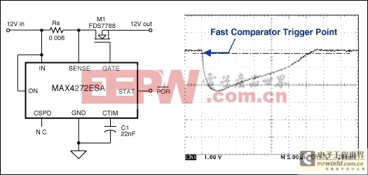
Figure 1. Typical hot-swap controller circuit exhibits a 30ms short-circuit current pulse of 400A peak.
The initial short-circuit current spike is limited only by circuit resistances1 during a period that includes the fast-comparator delay and the 30μs it takes to complete interruption of the short circuit by discharging M1's gate capacitance. The waveform recorded during a short circuit indicates a peak current of 400A (due to 2.4Vpk across Rs), decreasing to 100A in 28μs.
The short-circuit current duration can be limited to ≤ 0.5ms by adding a Darlington pnp transistor (Q1) to speed the gate discharge (Figure 2). D1 allows the gate to charge normally at turn-on, but at turn-off the controller's 3mA gate-discharge current is directed to the base of Q1. Q1 then acts quickly to discharge the gate, in ≤ 100ns. Thus, the high-current portion of the short circuit is limited to slightly more than the fast-comparator's delay time of 350ns.
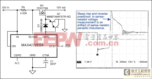
Figure 2. The addition of Q1 increases the gate-pulldown current, limiting the short-circuit current duration to less than 0.5ms.
The apparent reverse overshoot current and the steep rise seen in the waveforms of Figures 2 and 3 is created by parasitic series inductance in the sense resistor chip, and the leading-edge oscillation seen in Figure 3 is an artifact introduced by the oscilloscope ground lead.
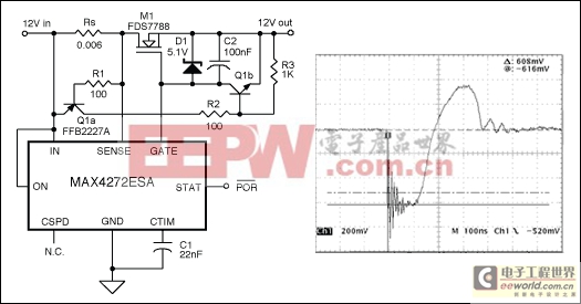
Figure 3. Hot-swap controller with fast limiting of short-circuit current peaks, and short-circuit waveform.
The circuit of Figure 3 can limit short-circuit current to ≈100A for 200ns. The pnp transistor Q1a, which is triggered when the voltage across RS reaches ≈600mV, drives the npn transistor Q1b to quickly discharge M1's gate capacitance. Quick triggering of the pnp transistor is aided by the steep voltage waveform, which in turn is a result of parasitic inductance in the sense-resistor.
C2 is connected between the gate and source of M1 to reduce the positive transient step voltage applied to the gate during a short circuit. Zener diode D1 reduces ID(ON) by limiting VGS to something less than the 7V available from the MAX4272. Although D1 is rated 5.1V when biased at 5mA, it limits VGS to ≈3.4V in this circuit because only 100mA of gate-charging current (zener bias current) is available from the IC. The limited VGS lowers ID(ON)—at some expense to RD(ON)—and allows a quicker turn off of M1. D1 and C2 can also be employed to some advantage in Figure 1 and Figure 2, to reduce ID(ON) during short circuits.
Either of the two circuits above can protect a backplane power source by minimizing the energy dissipated when a hot-swap-controlled circuit is shorted. The simpler circuit (Figure 2) dramatically shortens the short-circuit-current interval to somewhat less than 500ns, and the slightly more complex circuit (Figure 3) reduces the peak short-circuit current to 100A, as well as truncating the pulse width to less than 200ns. Either technique can be applied to most hot-swap controller circuits. Individual results vary2 according to the impedance of the power source, the impedance of the short circuit, and (especially) the quality and attack time of the short circuit itself.
1Source resistance, short-circuit quality, value of RS, MOSFET's RDS(ON), and MOSFET's ID(ON).
2Note that it is inordinately difficult to achieve a repeatable low-resistance short circuit by manual manipulation of a shorting bar. Careful layout and low-ESR capacitors are required to create a power source with very low ESR.
This design idea appeared in the May 27, 2004 issue of EDN.





評論