How to Reduce Reference Noise
Stacking multiple references will reduce LF noise. By using multiple voltage sources, each composed of a DC source and a noise source, the DC voltages increase linearly and the noise sources (if not correlated) sum geometrically in an RMS fashion. Adding four references, for example, each consisting of a VREF generator and a VNOISE generator, produces the following outputs:

The original ratio of noise voltage to DC reference voltage is divided in half.
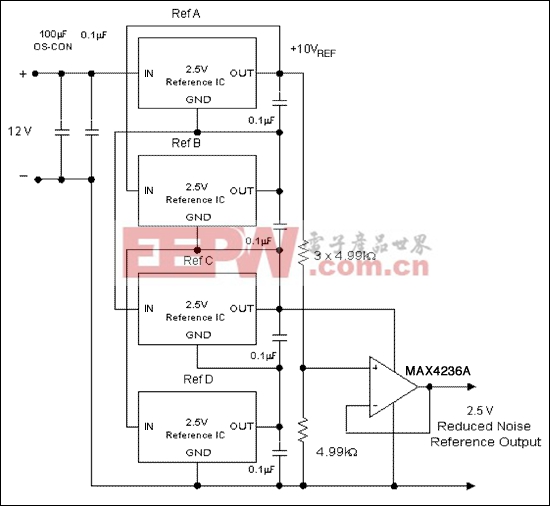
Figure 1 shows how to stack multiple references to generate a single, less noisy reference voltage. The resistors are parts of a high-stability metal-film network, and the op amp is selected for low noise, very low input-offset voltage, and low offset tempco.

Figure 1. Four 2.5V references are stacked to produce 10V. The output is then divided back to 2.5V, which reduces the noise voltage by half.
Two types of 2.5V voltage references can be used in the design. Table 1 and Table 2 show the noise voltages that result from use of either the MAX6037 or the MAX6143 reference. Each table shows the 0.1Hz-to-10Hz noise voltage for the four references individually, and for them in combination. (The dispersion in the ratios of RMS to peak-to-peak (P-P) values is due to some subjectivity in the method used to measure those P-P values.)
Table 1. Noise Voltage Measurements of the Circuit in Figure 1 Using the MAX6037 2.5V Voltage Reference
| Measurement Points | Noise (μVRMS) | Noise(μVP-P) |
| Reduced noise output(op amp, output to V-) | 1.0 | 10 |
| Across Reference A(OUTA to GNDA) | 1.9 | 20 |
| Across Reference B(OUTB to GNDB) | 1.6 | 19 |
| Across Reference C(OUTC to GNDC) | 1.7 | 20 |
| Across Reference D(OUTD to GNDD) | 2.7 | 30 |
Table 2. Noise Voltage Measurements of Figure 1 Circuit Using MAX6143 2.5V Voltage References
| Measurement Points | Noise (μVRMS) | Noise(μVP-P) |
| Reduced noise output(op amp, output to V-) | 0.27 | 2.2 |
| Across Reference A(OUTA to GNDA) | 0.52 | 4.7 |
| Across Reference B(OUTB to GNDB) | 0.60 | 4.8 |
| Across Reference C(OUTC to GNDC) | 0.50 | 4.3 |
| Across Reference D(OUTD to GNDD) | 0.55 | 4.7 |
As an additional benefit of this reference-stack arrangement, the portion of long-term drift due to noise will also be reduced.
A similar version of this article appeared as a Design Idea in the February 3, 2005 issue of EDN magazine.


評論